 | –≠–ª–µ–∫—Ç—Ä–æ–Ω–Ω—ã–π –∫–æ–º–ø–æ–Ω–µ–Ω—Ç: M14C04 | –°–∫–∞—á–∞—Ç—å:  PDF PDF  ZIP ZIP |
1/13
March 1999
M14C16
M14C04
Memory Card IC
16/4 Kbit Serial I≤C Bus EEPROM
s
Two Wire I
2
C Serial Interface
Supports 400 kHz Protocol
s
Single Supply Voltage (2.5 V to 5.5 V)
s
Hardware Write Control
s
BYTE and PAGE WRITE (up to 16 Bytes)
s
BYTE, RANDOM and SEQUENTIAL READ
Modes
s
Self-Timed Programming Cycle
s
Automatic Address Incrementing
s
Enhanced ESD/Latch-Up Behaviour
s
1 Million Erase/Write Cycles (minimum)
s
40 Year Data Retention (minimum)
s
5 ms Programming Time (typical)
DESCRIPTION
Each device is an electrically erasable program-
mable memory (EEPROM) fabricated with STMi-
croelectronics's High Endurance, Single
Polysilicon, CMOS technology. This guarantees
an endurance typically well above one million
Erase/Write cycles, with a data retention of
40 years. The memory operates with a power sup-
ply as low as 2.5 V.
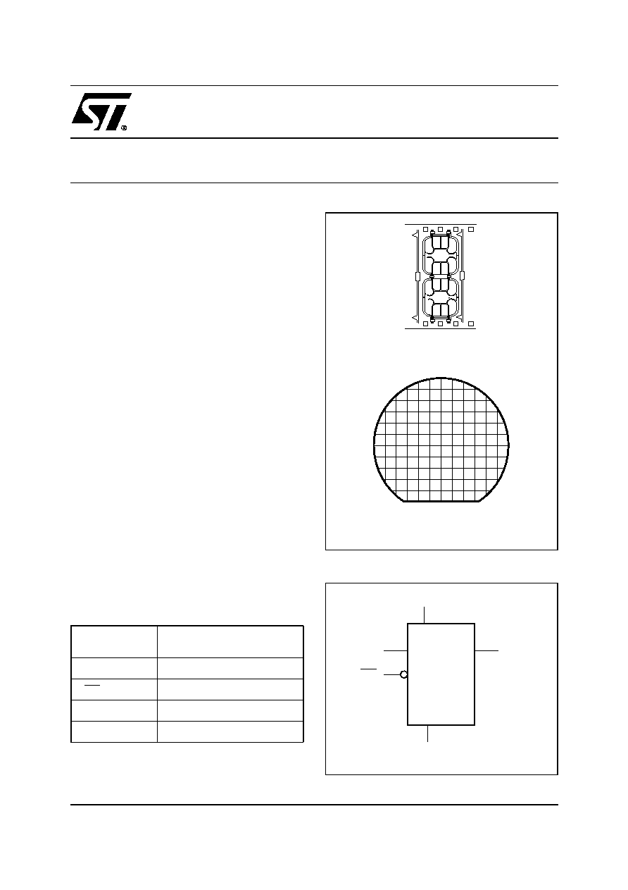
The M14C16 and M14C04 are each available in
wafer form (either sawn or unsawn) and in micro-
module form (on film).
Each memory is compatible with the I
2
C memory
standard. This is a two wire serial interface that
Figure 1. Logic Diagram
AI02217
SDA
VCC
M14xxx
WC
SCL
GND
Table 1. Signal Names
SDA
Serial Data/Address Input/
Output
SCL
Serial Clock
WC
Write Control
V
CC
Supply Voltage
GND
Ground
2
2
2
2
Micromodule (D20)
Wafer

M14C16, M14C04
2/13
uses a bi-directional data bus and serial clock. The
memory carries a built-in 7-bit unique Device Type
Identifier code (1010xxx, for the M14C16, and
101000x, for the M14C04, as shown in Table 3) in
accordance with the I
2
C bus definition. Only one
memory can be attached to each I
2
C bus.
The memory behaves as a slave device in the I
2
C
protocol, with all memory operations synchronized
by the serial clock. Read and write operations are
initiated by a START condition, generated by the
bus master. The START condition is followed by
the Device Select Code which is composed of a
stream of 7 bits (1010xxx, for the M14C16, and
101000x, for the M14C04, as shown in Table 3),
plus one read/write bit (R/W) and is terminated by
an acknowledge bit.
When writing data to the memory, the memory in-
serts an acknowledge bit during the 9
th
bit time,
following the bus master's 8-bit transmission.
When data is read by the bus master, the bus
master acknowledges the receipt of the data byte
in the same way. Data transfers are terminated by
a STOP condition after an Ack for WRITE, and af-
ter a NoACK for READ.
Power On Reset: V
CC
Lock-Out Write Protect
In order to prevent data corruption and inadvertent
write operations during power up, a Power On Re-
set (POR) circuit is included. The internal reset is
held active until the V
CC
voltage has reached the
POR threshold value, and all operations are dis-
abled ≠ the device will not respond to any com-
mand. In the same way, when V
CC
drops from the
operating voltage, below the POR threshold value,
all operations are disabled and the device will not
respond to any command. A stable and valid V
CC
must be applied before applying any logic signal.
SIGNAL DESCRIPTION
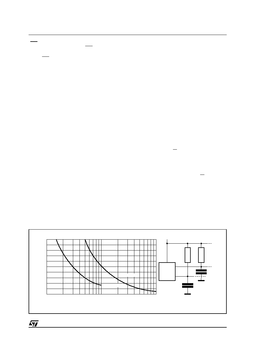
Serial Clock (SCL)
The SCL input pin is used to synchronize all data
in and out of the memory. A pull up resistor can be
connected from the SCL line to V
CC
. (Figure 3 in-
dicates how the value of the pull-up resistor can be
calculated).
Serial Data (SDA)
The SDA pin is bi-directional, and is used to trans-
fer data in or out of the memory. It is an open drain
output that may be wire-OR'ed with other open
drain or open collector signals on the bus. A pull
up resistor must be connected from the SDA bus
to V
CC
. (Figure 3 indicates how the value of the
pull-up resistor can be calculated).
Write Control (WC)
The hardware Write Control contact (WC) is useful
for protecting the entire contents of the memory
from inadvertent erase/write. The Write Control
signal is used to enable (WC=V
IL
) or disable
Figure 2. D20 Contact Connections
AI02168
VCC
GND
SCL
SDA
WC
Table 2. Absolute Maximum Ratings
1
Note: 1. Except for the rating "Operating Temperature Range", stresses above those listed in the Table "Absolute Maximum Ratings" may
cause permanent damage to the device. These are stress ratings only, and operation of the device at these or any other conditions
above those indicated in the Operating sections of this specification is not implied. Exposure to Absolute Maximum Rating condi-
tions for extended periods may affect device reliability. Refer also to the ST SURE Program and other relevant quality documents.
2. MIL-STD-883C, 3015.7 (100 pF, 1500
)
3. EIAJ IC-121 (Condition C) (200 pF, 0
)
Symbol
Parameter
Value
Unit
T
A
Ambient Operating Temperature
0 to 70
∞C
T
STG
Storage Temperature
Wafer form
Module form
-65 to 150
-40 to 120
∞C
V
IO
Input or Output range
-0.6 to 6.5
V
V
CC
Supply Voltage
-0.3 to 6.5
V
V
ESD
Electrostatic Discharge Voltage (Human Body model)
2
4000
V
Electrostatic Discharge Voltage (Machine model)
3
400
V
3/13
M14C16, M14C04
(WC=V
IH
) write instructions to the entire memory
area. When unconnected, the WC input is internal-
ly read as V
IL
and write operations are allowed.
When WC=1, Device Select and Address bytes
are acknowledged, Data bytes are not acknowl-
edged.
Please see the Application Note
AN404
for a more
detailed description of the Write Control feature.
DEVICE OPERATION
The memory device supports the I
2
C protocol, as
summarized in Figure 4. Any device that sends
data on to the bus is defined to be a transmitter,
and any device that reads the data to be a receiv-
er. The device that controls the data transfer is
known as the master, and the other as the slave.
A data transfer can only be initiated by the master,
which will also provide the serial clock for synchro-
nization. The memory device is always a slave de-
vice in all communication.
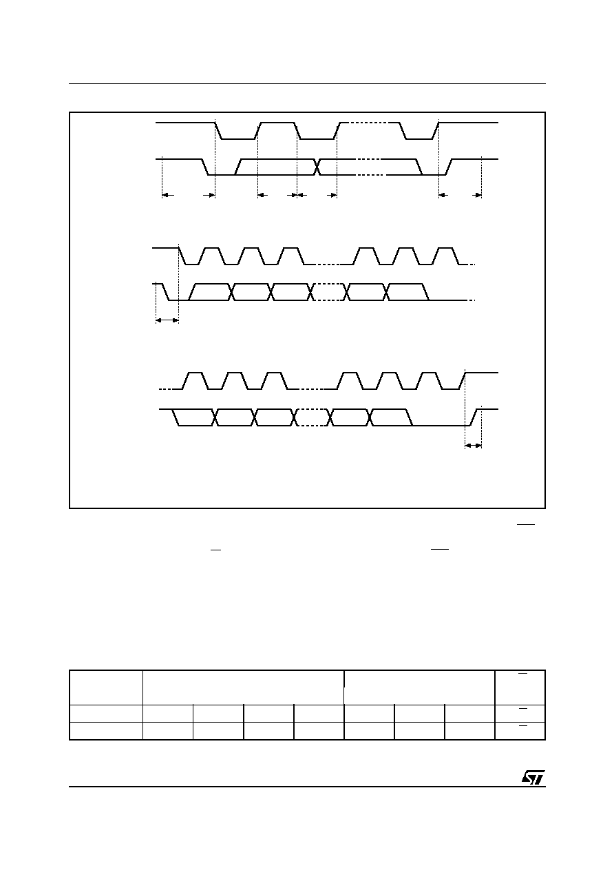
Start Condition
START is identified by a high to low transition of
the SDA line while the clock, SCL, is stable in the
high state. A START condition must precede any
data transfer command. The memory device con-
tinuously monitors (except during a programming
cycle) the SDA and SCL lines for a START condi-
tion, and will not respond unless one is given.
Stop Condition
STOP is identified by a low to high transition of the
SDA line while the clock SCL is stable in the high
state. A STOP condition terminates communica-
tion between the memory device and the bus mas-
ter. A STOP condition at the end of a Read
command, after (and only after) a NoACK, forces
the memory device into its standby state. A STOP
condition at the end of a Write command triggers
the internal EEPROM write cycle.
Acknowledge Bit (ACK)
An acknowledge signal is used to indicate a suc-
cessful data transfer. The bus transmitter, either
master or slave, will release the SDA bus after
sending 8 bits of data. During the 9
th
clock pulse
period the receiver pulls the SDA bus low to ac-
knowledge the receipt of the 8 data bits.
Data Input
During data input, the memory device samples the
SDA bus signal on the rising edge of the clock,
SCL. For correct device operation, the SDA signal
must be stable during the clock low-to-high transi-
tion, and the data must change
only
when the SCL
line is low.
Memory Addressing
To start communication between the bus master
and the slave memory, the master must initiate a
START condition. Following this, the master sends
8 bits to the SDA bus line (with the most significant
bit first). These bits represent the Device Select
Code (7 bits) and a RW bit.
The seven most significant bits of the Device Se-
lect Code are the Device Type Identifier, according
to the I
2
C bus definition. For the memory device,
the seven bits are fixed as shown in Table 3.
The 8
th
bit is the read or write bit (RW). This bit is
set to `1' for read and `0' for write operations. If a
match occurs on the Device Select Code, the cor-
responding memory gives an acknowledgment on
the SDA bus during the 9
th
bit time. If the memory
does not match the Device Select code, it will de-
select itself from the bus, and go into stand-by
mode.
Figure 3. Maximum R
L
Value versus Bus Capacitance (C
BUS
) for an I
2
C Bus
AI01665
VCC
CBUS
SDA
RL
MASTER
RL
SCL
CBUS
100
0
4
8
12
16
20
CBUS (pF)
Maximum RP value (k
)
10
1000
fc = 400kHz
fc = 100kHz
M14C16, M14C04
4/13
Write Operations
Following a START condition the master sends a
Device Select code with the RW bit set to '0', as
shown in Table 4. The memory acknowledges it
and waits for a byte address, which provides ac-
cess to the memory area. After receipt of the ad-
dress, the memory again responds with an
acknowledge and waits for the data byte. Writing
in the memory may be inhibited if input pin WC is
taken high.
Any write command with WC=1 (during a period of
time from the START condition until the end of the
address) will not modify the memory content and
will NOT be acknowledged on data bytes, as
shown in Figure 5.
Figure 4. I
2
C Bus Protocol
SCL
SDA
SCL
SDA
SDA
START
CONDITION
SDA
INPUT
SDA
CHANGE
AI00792
STOP
CONDITION
1
2
3
7
8
9
MSB
ACK
START
CONDITION
SCL
1
2
3
7
8
9
MSB
ACK
STOP
CONDITION
Table 3. Device Select Code
1
Note: 1. A10, A9 and A8 correspond to the most significant bits of the memory array address word.
Device Code
Chip Enable
RW
b7
b6
b5
b4
b3
b2
b1
b0
M14C16 Select
1
0
1
0
A10
A9
A8
RW
M14C04 Select
1
0
1
0
0
0
A8
RW
5/13
M14C16, M14C04
Figure 5. Write Mode Sequences with WC=1
STOP
START
BYTE WRITE
DEV SEL
BYTE ADDR
DATA IN
WC
START
PAGE WRITE
DEV SEL
BYTE ADDR
DATA IN 1
DATA IN 2
WC
DATA IN 3
AI02803B
PAGE WRITE
(cont'd)
WC (cont'd)
STOP
DATA IN N
ACK
ACK
NO ACK
R/W
ACK
ACK
NO ACK
NO ACK
R/W
NO ACK
NO ACK
Byte Write
In the Byte Write mode, after the Device Select
code and the address, the master sends one data
byte. If the addressed location is write protected by
the WC pin, the memory replies with a NoACK,
and the location is not modified. If, instead, the WC
pin has been held at 0, as shown in Figure 6, the
memory replies with an ACK. The master termi-
nates the transfer by generating a STOP condi-
tion.
Page Write
The Page Write mode allows up to 16 bytes to be
written in a single write cycle, provided that they
are all located in the same 'row' in the memory:
that is the most significant memory address bits
(b10-b4 for the M14C16 and b8-b4 for the
M14C04) are the same. The master sends from
one up to 16 bytes of data, each of which is ac-
knowledged by the memory if the WC pin is low. If
the WC pin is high, each data byte is followed by a
NoACK and the location is not modified. After each
byte is transferred, the internal byte address coun-
ter (the four least significant bits only) is incre-
mented. The transfer is terminated by the master
generating a STOP condition. Care must be taken
to avoid address counter 'roll-over' which could re-
sult in data being overwritten. Note that, for any
byte or page write mode, the generation by the
master of the STOP condition starts the internal
memory program cycle. This STOP condition trig-
gers an internal memory program cycle only if the
STOP condition is internally decoded immediately
after the ACK bit; any STOP condition decoded
out of this "10
th
bit" time slot will not trigger the in-
ternal programming cycle. All inputs are disabled
until the completion of this cycle and the Memory
will not respond to any request.
Minimizing System Delays by Polling On ACK
During the internal write cycle, the memory discon-
nects itself from the bus, and copies the data from
its internal latches to the memory cells. The maxi-
mum write time (t
w
) is indicated in Table 5, but the